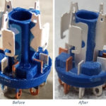
Crystal Mark has refined methodology to confirm the feasibility of an application, and to develop a validated process that can be carried out consistently for a project of any size.
R & D: Process Development
Step One: Define the problem to be solved.
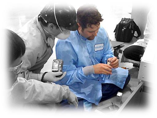
The Crystal Mark team works closely with the customer to understand the objective for the application, starting with sample parts or technical drawings, and detailed discussion.
Step Two: Understand the technology.
The Crystal Mark team draws on its extensive experience while developing the process for the customer’s application: a company specialty for over 50 years. The specific industry regulations and conformance requirements are taken into account during this process.
Example applications domains:
- Semiconductor: manufacturing of devices, MEMS, cleaning of inside chambers
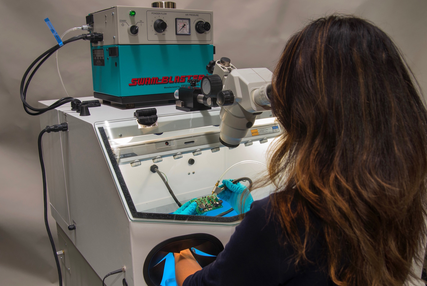
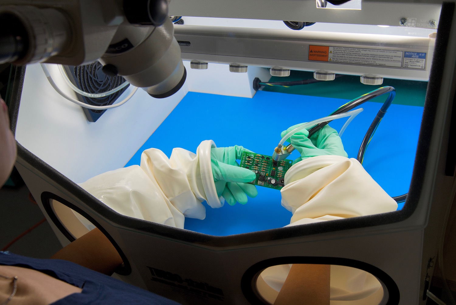
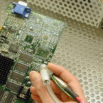
- Electronics circuits: selective removal of conformal coating
- Medical applications: electronic circuit boards, surface finishing, deburring
- Paleontology
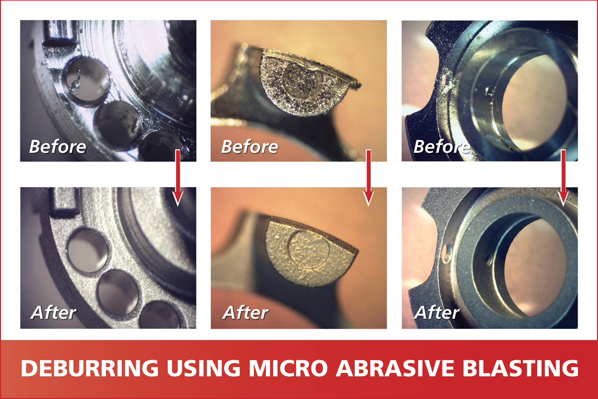
- Machining – surface finishing, cleaning, deburring – industrial parts
- Removal of flash off of packages
Crystal Mark is able to develop a customized micro abrasive process for virtually any industrial discipline where micro abrasive blasting is relevant.
Step Three: Confirm, validate feasibility.
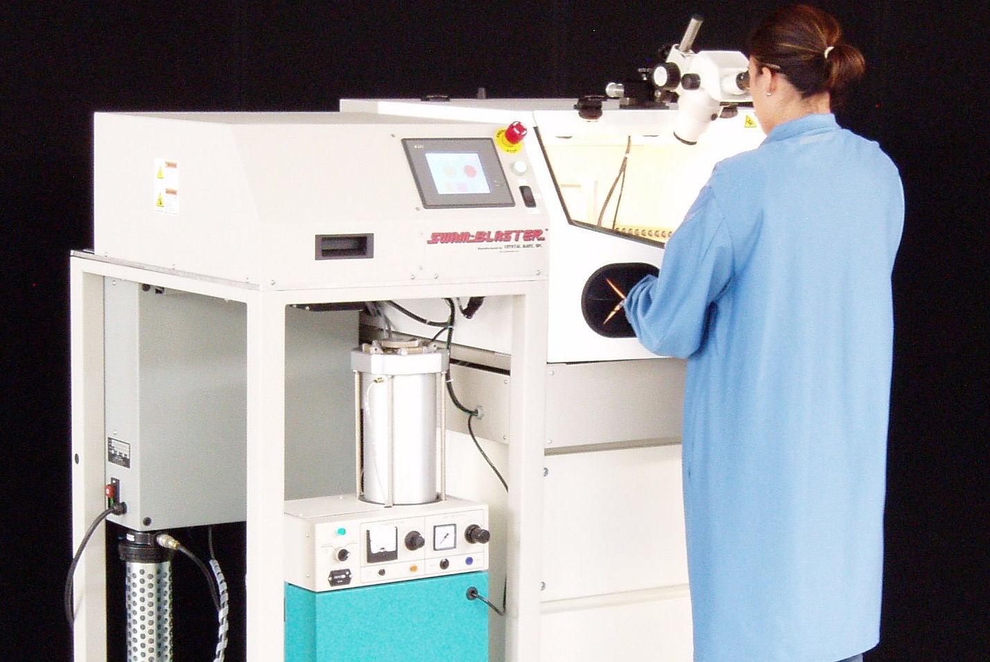
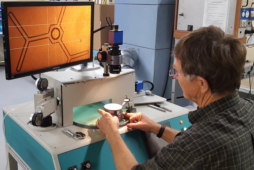
Crystal Mark is able to work on the customer’s sample using an in-house Abrasive Lab, and provide proof of concept to confirm that the customer’s application can be achieved using micro abrasive blasting. It helps to have drawing of parts, critical dimensions, etc. with the samples for positive validation of the application feasibility.
Step Four: Recommendations, Proposed Plan.
Once the application feasibility is confirmed, the Crystal Mark team can give a recommended design process, or suggest a course of R & D for process optimization.
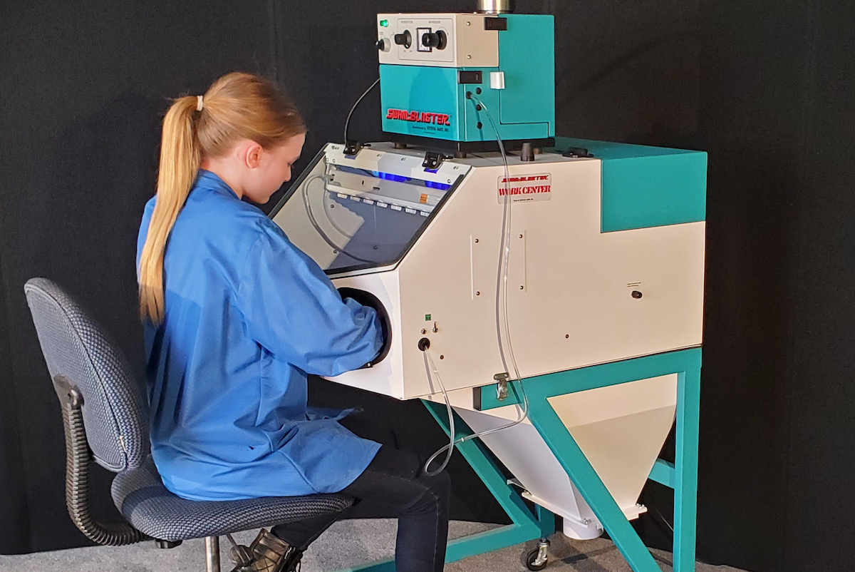
- Customers have a choice either to use Crystal Mark’s Abrasive Lab and Job Shop to get the work done or to get the required equipment, accessories, and abrasives to execute the application in their own facility.
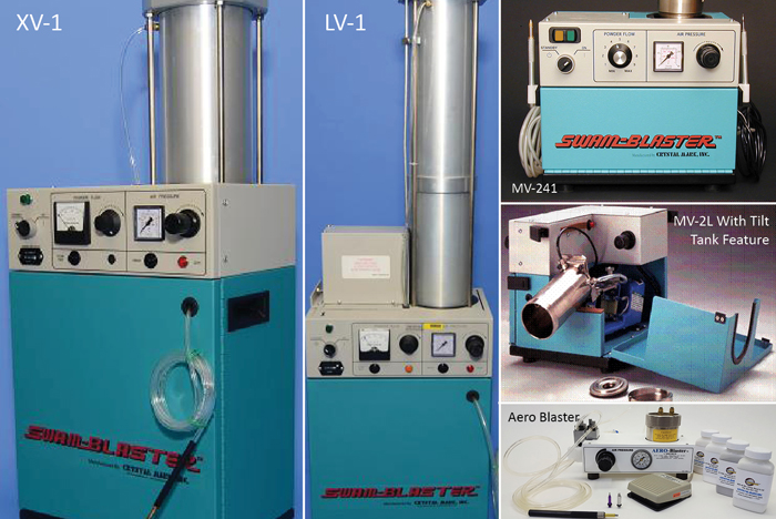
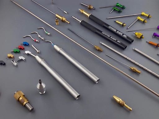
- Crystal Mark has flexibility and options with products, abrasives, as well as accessories to cater to the customer’s specific application requirements. Crystal Mark provides required training for consistent results using the products.
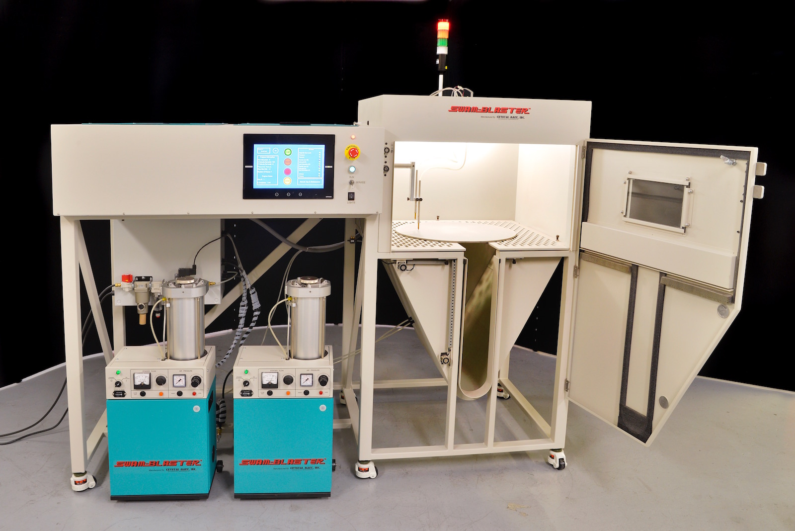
- For larger-scale applications, Crystal Mark is able to work closely with the customer to develop fully automated systems. Crystal Mark uses its extensive manufacturing capability and trusted supply chain partners to deliver a fully automated solution.

