Controlled Erosion

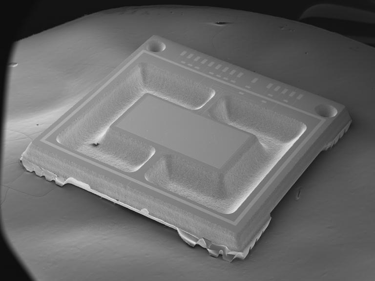
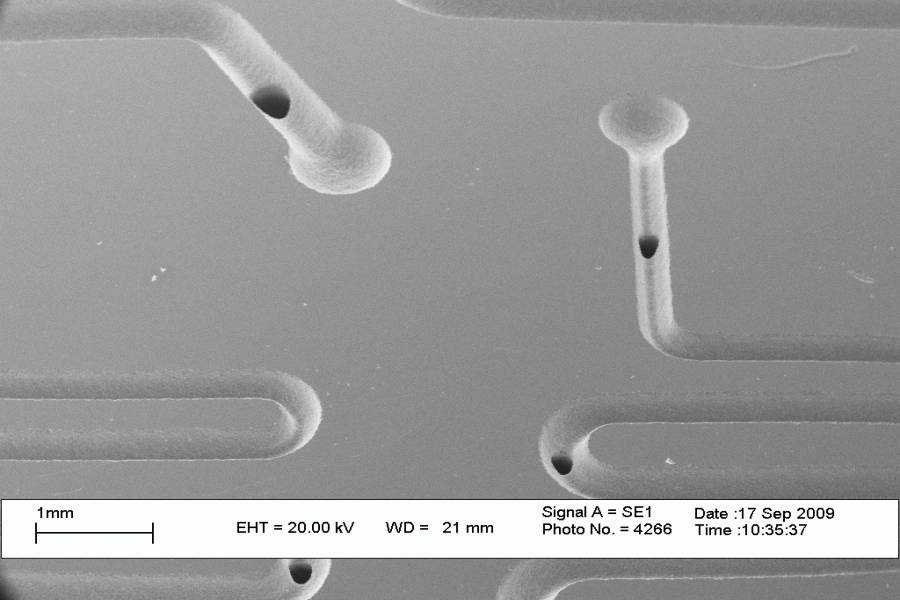
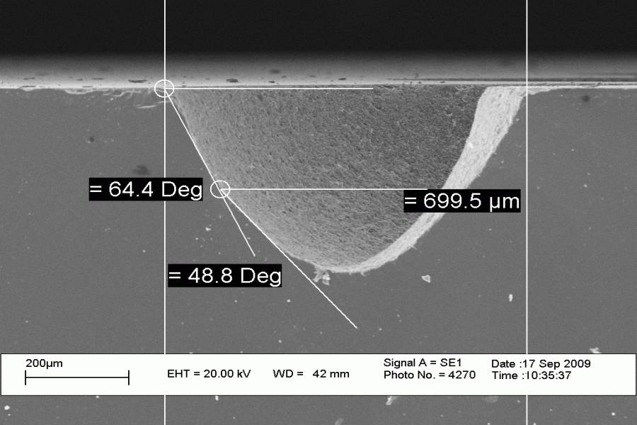
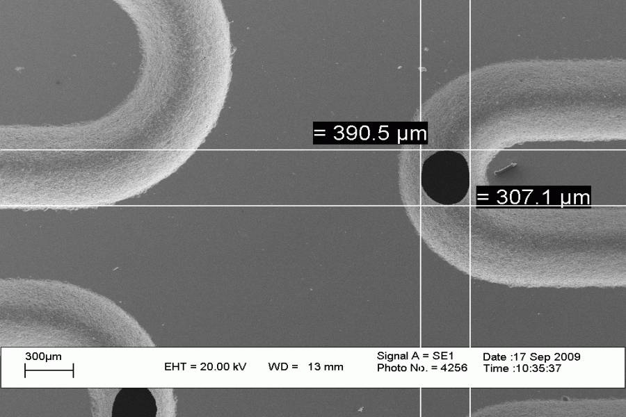
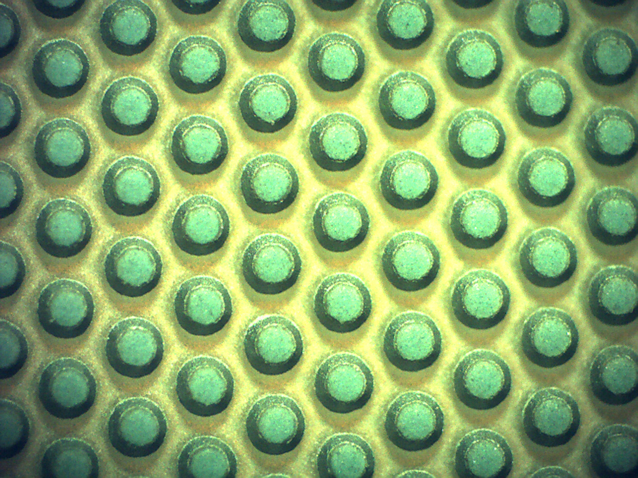
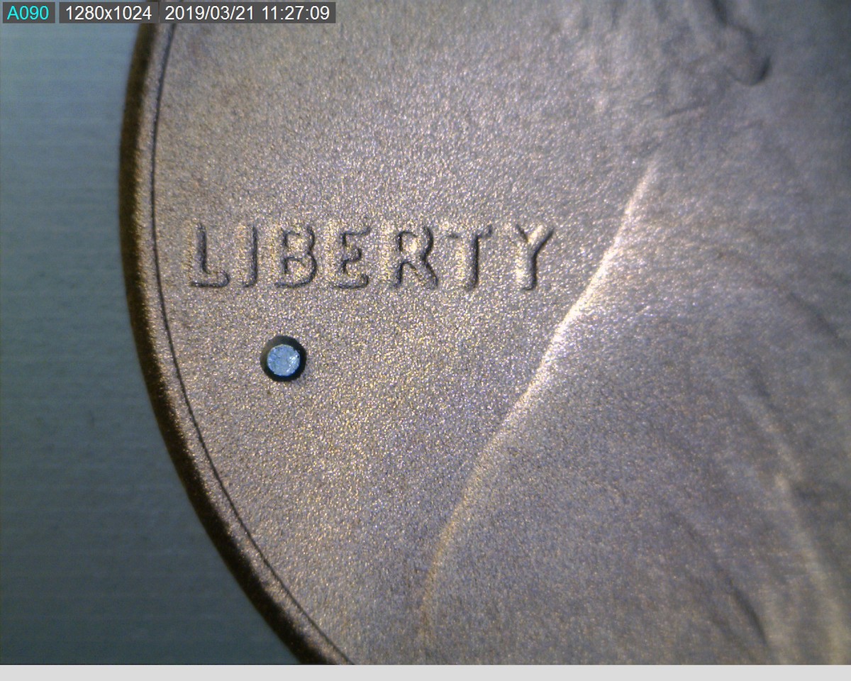
Crystal Mark’s micro-abrasive processing technology has the required precision to carry out a range of “controlled erosion” or mechanical abrasive etching applications. In many cases, the process uses a mask to etch away the substrate areas that are not protected selectively.

  • Crystal Mark, Inc. has a proven track record for developing successful controlled erosion processes for ceramics, glass, semiconductor, and other brittle materials. Customers get comparable consistency, repeatability, and accuracy compared to laser etching without slags, recast, or thermal stress.
  • The team works closely with customers to understand their requirements and suggest the most appropriate masking material and abrasive for the micro sandblasting process.
  • Customers have the option to get their job work done using Crystal Mark’s in-house micro-abrasive lab. Alternatively, customers can acquire the SWAM® micro sandblasting system, customized for their specific requirements.

With complete mastery of the micro-blasting process variables, customers get unparalleled accuracy, precision, and consistency. When required, customers can also get fully automated systems, leveraging Crystal Mark’s in-house manufacturing capabilities.

MICRO ABRASIVE PROCESSING TECHNOLOGY FOR MEMS

Crystal Mark’s R & D team has successfully developed several micromachining processes that selectively etch away parts of a substrate. The technology is used on many Micro-Electro-Mechanical Systems (MEMS) to integrate mechanical elements, sensors, and electronics for various applications.

Wafer Micro-machining and Coring

Silicon Wafer Micro-machining and Coring

Micro Abrasive Blasting Technology for MEMS

Micro Abrasive Blasting Technology for MEMS

Micro Abrasive Blasting Technology for MEMS

Micro Abrasive Blasting Technology for MEMS

Micro Abrasive Blasting Technology for MEMS

Micro Abrasive Blasting Technology for MEMS

Example Applications:

  • Produce complex electrical, mechanical, thermal, optical-mechanical, fluidic, magnetic structures and devices
  • Etching patterns
  • Fiducial targets
  • Interconnect vias or through holes and pockets into all types of semiconductor materials
  • Piezoceramics such as PZT (Lead Zirconate Titanate) or Barium Titanate – develop ultrasonic transducers and ceramic capacitors
  • Controlled etching on the substrate materials such as Gallium Arsenide, Sapphire, Silicon Carbide

MICRO MACHINING – MANUFACTURING OF MESA DIODES

Crystal Mark, Inc. has a very well-developed process to manufacture mesa diodes using specific masking materials.

Images below show microscopic images of mesa diodes manufactured using the SWAM® C1216 belt abrader. The top of the mesa in this example is 0.019” (482 microns), and the bottom is 0.027” (684 microns).

Mesa Diodes Manufacturing | Microscopic Image - the top of the mesa 0.019” (482 microns) and the bottom is 0.027” (684 microns)

Mesa Diodes Manufacturing | Microscopic Image – the top of the mesa 0.019” (482 microns) and the bottom is 0.027” (684 microns)

Diode on a Penny

SILICON WAFERS CORING, EDGE-BEVELING

Crystal Mark’s micro-abrasive blasting technology has the required precision and control to core all types of wafers required by semiconductor manufacturers, biomedical engineering companies, aerospace companies, electronics manufacturers, etc.