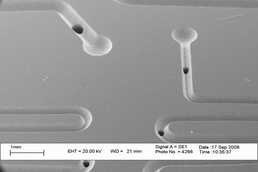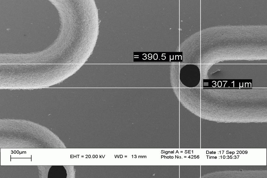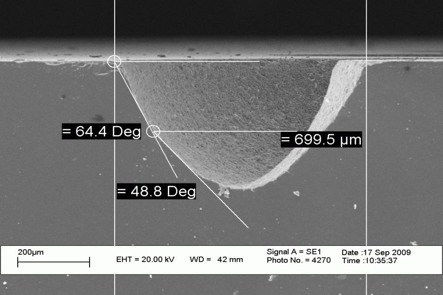

Wafer Micro-machining and Coring
Crystal Mark’s micro-abrasive blasting technology has the required precision and control to core all types of wafers required by semi-conductor manufacturers and biomedical engineering companies. It also has other applications, including etching patterns, features, fiducial targets, vias, or holes and pockets into all types of semiconductor materials.