What NASA Thinks About Us
EVALUATION OF ESD EFFECTS DURING REMOVAL OF CONFORMAL
COATINGS USING MICRO ABRASIVE BLASTING
Harry Shaw
NASA/GSFC, Greenbelt, MD
Nitin Parekh, Carroll Clatterbuck
Unisys/NASA, Lanham, MD
Felix Frades
HEI/NASA, Lanham, MD
Abstract
This report details the results and conclusions of an experimental evaluation of a micro abrasive blasting technique to remove urethane and parylene conformal coatings from printed wiring assemblies. This technique is being evaluated as a replacement for solvent based systems. The SWAM BLASTER coating removal system from Crystal Mark, Inc. was used. Four blast medias were evaluated using a total of 20 printed wiring assemblies. The effectiveness of the microblasting technique was evaluated to determine the electrostatic potential generated at the surface and any visible board damage. The microblaster effectively removed the conformal coatings from all printed wiring assemblies evaluated. However, the concerns of electrostatic potential generation and the effects of a number of variables which were not addressed in this study, needs further research prior to being acceptable for space flight applications.
Background
Conformal coatings are required on printed wiring assemblies (PWAs) used for space light applications to provide protection and to extend the life of the assemblies in harsh environments. There are four major types of coating materials, each developed to suit specific applications. These are: acrylics, urethanes, silicones and parylenes. Depending upon the type of coating material and product requirements, conformal coating may be applied by dipping, brushing, spraying, dispensing or chemical vapor deposition. In order to rework or repair parts on PWAs, the conformal coating must be removed, either entirely or in specific areas. The most commonly used methods for removal involve thermal, chemical, mechanical and micro abrasive processes. Recent environmental regulations such as the Montreal Protocol and Clean Air Act have had a significant impact on solvent based conformal coating removal processes, particularly with regard to control of volatile organic compounds (VOCs) and ozone depleting chemicals (ODCs). Equipment suppliers for coating removal systems have responded by developing environmentally acceptable methods. The micro abrasive blasting technique offers a fast, cost-effective, easy to control and environmentally friendly non-solvent based method to remove conformal coatings. The system can remove conformal coatings from a single test node, an axial leaded component, a through-hole integrated circuit (IC), a surface mount component (SMC) or an entire printed circuit board (PCB). In the micro abrasive blasting process, a precise mixture of dry air or an inert gas and an abrasive media is propelled through a tiny nozzle attached to a stylus which is either hand held or mounted on an automated system. This allows the mixture to be pinpointed at the target area of the conformal coating to be removed. A vacuum system continuously removes the used materials and channels them through a filtration system for disposal. The process is conducted within an enclosed anti-static chamber and features grounding devices to dissipate electrostatic potential. Micro abrasive systems inherently generate static electricity as the high velocity particles impinge on the surfaces. The voltage generated at the area of impact can cause electrostatic discharge (ESD) damage to the parts and electrical circuits on a PWA. The current trend in the electronics industry towards higher speed, greater packaging density and lower power consumption has increased static sensitivity so that new techniques emerging in the field of coating technology need more stringent attention than ever before. An ideal blast media in a coating removal process would be the one which will not generate voltage greater than the ESD susceptibility of a particular device on a PWA or damage the board assembly, and is environmentally acceptable.
Conformal Coating Removal
Methodology
The objective of this study is to determine the effectiveness of the micro abrasive blasting technique to remove the conformal coatings from printed circuit boards and assemblies. This evaluation includes determination of the level of electrostatic voltage by measuring the surface voltage generated at the point of contact. It also includes assessing any physical damage caused by the technique. The experimental characterization includes the effects of variables such as type of conformal coating, cutting media, and system parameters on the conformal coating removal process.
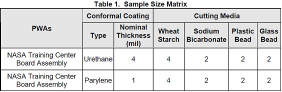
Two types of conformal coatings were evaluated. These included urethane and parylene (parylene type C) conformal coatings with 4 mil and 1 mil nominal thicknesses respectively. The PWAs were non-functional. A total of four blast medias were selected. These included: wheat starch, sodium bicarbonate, plastic beads and glass beads.
A SWAM BLASTER Model MV-1 made by Crystal Mark, Inc. Glendale, California was used throughout this study. A Monroe Electronics Model 244 Isoprobe Electrostatic Voltmeter was used to monitor ESD voltages generated at the surfaces. This electrostatic voltmeter used an end-viewing miniature probe (Model 1017) with inert gas purging capability. Cleaninert gas is purged through the sensing aperture preventing contamination by the blast medias in the vicinity of the electrode for greater stability of measurement. The probe measures the surface voltage with high accuracy (0.1%) and a test response speed < 3mS throughout a range of ± 3 kilovolts.
The evaluation was performed at the Materials Engineering Laboratory, NASA/GSFC in Greenbelt, Maryland.
Experimental Plan
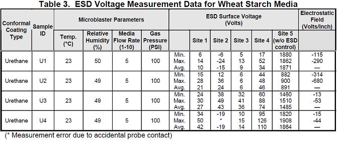
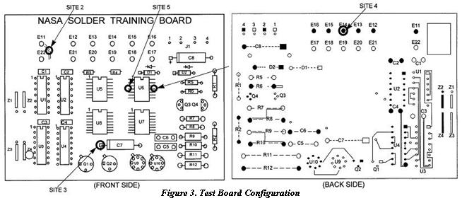
A total of 20 non-functional PWAs were selected for this evaluation. All PWAs were double sided, 75mm x 125 mm (3″ x 5″) FR4 laminate. These PWAs have been designed for the use by the NASA Training Center for training in hand soldering, surface mount attachment,cleaning and conformal coating applications. This configuration provided a variety of pad geometries and traces adjacent to the blast sites and in close proximity to through-hole parts, flat packs, and other discrete devices (see figure 2 and 3).
A total of five blast sites were selected for monitoring ESD voltage (see figure 2 and 3).
These included:
Experimental Matrix
A total of 20 PWAs were coated with urethane and parylene conformal coatings; ten each. All four blast medias were procured from Crystal Mark, Inc. The specifications of these are listed below:
All test PWAs were fabricated in accordance with NASA handbooks NHB5300.4 (3A-2) on soldering and NAS 5300.4 (3M) covering surface mount technology. All soldering operations and cleaning were performed at the NASA Training Center located at Unisys facility in Lanham, Maryland.
Cleaning
All PWAs were spray cleaned using 1:1 parts by volume of ethyl alcohol/heptane. The cleaning was performed in accordance with the Materials Processing Document – “Conformal Coating and Staking of Printed Wiring Boards Using a Room Temperature Curing Urethane Resin” (MPD S-313-008, Rev. C).
A. Urethane – A total of 10 PWAs were coated with urethane conformal coating. The resin formulation included Uralane 5750LV-A, Uralane 5750LV-B and a mixture of toluene and methyl ethyl ketone (MEK) solvents. The urethane conformal coating was applied to the front and back sides of the PWAs using a spray method in accordance with MPD S-313-008, Rev. C. The process parameters were adjusted to achieve a nominal coating thickness of 0.004″. After a 7 day cure period at ambient conditions, a visual inspection was performed on all PWAs.
B. Parylene – The parylene conformal coating was applied by a chemical vapor deposition process. The raw material for this process is di-paraxylelene, which is a dimer composition. The system used for parylene conformal coating deposition was a Vapor Deposition Coater from Paratronix, Inc., Attleboro, Massachusetts.
A total of 10 PWAs were loaded into the deposition chamber. The dimer was placed in a glass tube at the opposite end of the deposition chamber. As the dimer vaporizes from a solid to a vapor state it moves into the pyrolysis zone which is maintained at 680°C with a 40 micron vacuum. With these conditions, the dimer cleaves into monomers which reform as a long chain polymer and deposit on the surface of the PWA. A cold trap maintained at -90°C is used to prevent parylene from depositing in the vacuum pump and to prevent backstreaming of pump oil into the chamber.The process parameters were set to achieve a nominal 0.001″ parylene conformal coating thickness.
Conformal Coating Removal System
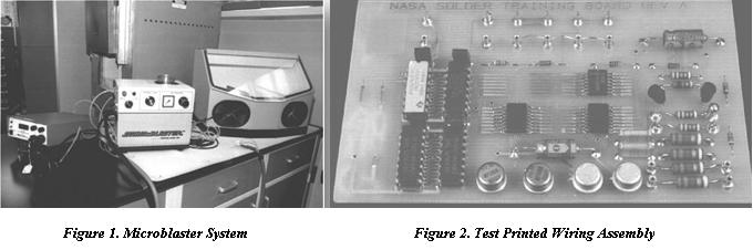
The system used for the conformal coating removal study was a SWAM BLASTER Model MV-1 micro blasting machine from Crystal Mark, Inc. . The model MV-1 is a manual system. The primary components of the system include a microblast unit, a work chamber, a gas dryer, an ESD point ionizer, a dust collector and a source of dry compressed air or an inert gas. The system design allows easy access and flexibility for pressure regulation, media flow control, nozzle replacements and orifice plate changes.During manual operation, a mixture of micro abrasive media and compressed gas is propelled through a specially designed hand held nozzle. The abrading process is accomplished by introducing a precise amount of finely graded powder (media) into a stream of compressed gas which can be controlled by a foot switch.The SWAM BLASTER system features a statically controlled work chamber for the protection of ESD sensitive parts. The system has a point ionizer which generates a balanced flow of positive and negative ions. It has a specially designed nozzle which couples the ions directly into the abrasive stream. By combining ESD neutralization directly into the abrasive pathway, the potential for ESD damage is minimized. Without the point ionizer, ESD voltages in excess of 3000 volts are realized. The work chamber is constructed of conductive laminate. All elements of the system including inside chamber surfaces, point ionizer, media, PWAs and the operator are connected to a common ground to ensure that they are at the same potential. The general specifications for the system are the following:
Figure 1 shows the Microblaster System.
Electrostatic Discharge Voltage Measurement
Electrostatic Voltmeter
In order to measure ESD voltage generated during micro blasting, a high accuracy, non-contacting electrostatic voltmeter (EVM) manufactured by Monroe Electronics was used. The Monroe Electronics Model 244 Isoprobe EVM measures a surface potential with 99.9% or better accuracy regardless of probe-to-surface spacing on sites as small as 0.1″ (2.5mm) diameter. The EVM functions by means of a high voltage amplifier which automatically drives the probe to the same potential as that of the surface under measurement. By monitoring the output of the amplifier, an accurate indication of an unknown ESD potential can be achieved.
Electrostatic Fieldmeter
A Model 709 static sensor from 3M Corporation was used to monitor the electrostatic field within the work chamber. This portable sensor did not have high accuracy and was used to get a general indication of the electrostatic field present. The sensor was placed within the work chamber approximately 10″ from the probe.
Process Description
The conformal coating removal experiments were conducted for two types of coatings and four blast medias. The following are the key variables involved in the conformal coating removal process:
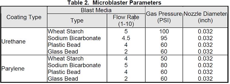
Since the type of blast media is the most important variable, the microblaster parameters such as media flow rate, gas pressure and coating removal time were optimized for each media and type of conformal coating. The nozzle parameters including the size, shape of orifice, distance from the PWA and angle of impingement were kept constant throughout the study.The microblaster was effective in removing both types of coatings within 30 seconds inmost cases. It was observed during the trial runs that as the media blasted through the coating, the surface ESD voltage increased. The ESD voltage peaked when the media hits pad or PWB surface. The primary goal of this study was to monitor the level of surface ESD generated during the coating removal process. Therefore, all measurements were taken instantaneously (within a few seconds) at the end of the coating removal. No attempt was made to monitor the rate of ESD voltage decay after the removal of the coating.Table 2 shows the optimized system parameters used for the removal of urethane and parylene conformal coatings.
Coating Removal Procedure
At the beginning of each run, all ESD precautions were in effect including grounding the equipment, operator and all elements of the work chamber to a common ground. The point ionization device was used throughout the process except when purposely taking measurements without it. The microblaster reservoir was filled completely with the appropriate media. The blast media was predryed at 100°C for 24 hours before use. The microblaster parameters were set to the optimized values as described in Table 2.The EVM probe was mounted on a stationary fixture with a spacer assembly so that the PWA could be positioned in front of the probe without surface contact. This ensured that all measurements could be taken at 3mm from the blast site irrespective of the location. The media flow was activated by a foot switch. In order to achieve high cutting speed and uniform removal of the conformal coating, the tip of the nozzle had to be positioned approximately an inch from the blast site and at an angle between 45 and 90 degrees from the PWB surface.At each site a 20 – 50 square mm area (5-8 mm diameter) was blasted until the conformal coating was completely removed. The total removal time ranged from 10 – 30 seconds for the pad and trace areas and 30 – 60 seconds for the solder joint areas. At the completion of the conformal coating removal the surface voltage measurements were taken within a few seconds. This method allowed a quick and repeatable measurement of surface voltages before the electrostatic charge could dissipate. All PWAs were microscopically inspected (10-40X) for any surface damage.
Results and Discussion
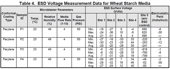
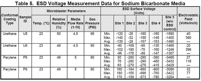
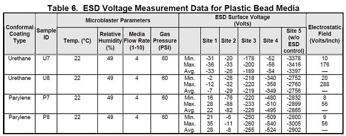
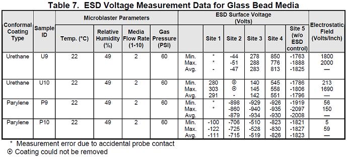
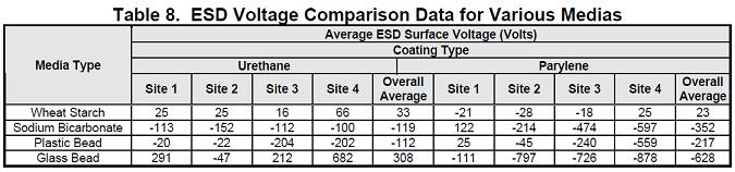
The experimental results of the study are presented in Tables 3 through 8.Tables 3 and 4 present the ESD surface voltage measurement data for the removal of urethane and parylene conformal coatings respectively for wheat starch media. The ESD surface voltages are reported as minimum, maximum and average measurement values. The data for site 5 shows the surface voltages measured without the use of a point ionizer for ESD control.
The cutting performance of the various blast medias showed mixed results. The microblaster parameters were optimized for media flow rate and gas pressure, however the effect of other factors such as nozzle parameters (orifice size and shape) and particle size variation for each media were not considered in this study. The main area of focus of this experimental study was ESD voltage generation during microblasting. The following observations describe the characteristics of the various medias evaluated.
Crystal Mark’s wheat starch (carbo-blast) media is specially developed for conformal coating removal in ESD sensitive applications. This media is water soluble, biodegradable and considered environmentally friendly. It had an average particle size of 120 micron and showed good flow without any nozzle clogging problems.
Both types of coatings could be easily removed relatively quickly without any visible damage or penetration into the PWB surface. The total time of removal at each site was less than 20 seconds for urethane and less than 10 seconds for parylene. In general, the removal was quicker and more uniform in the pad/trace areas compared to the solder joint areas. This media generated an average ESD surface voltage ranging from 16-66 volts for urethane and less than 30 volts for the removal of parylene.
The data from the voltage measurements when ESD control was not used showed interesting results proving the advantage of using a point ionizer. These measurements were taken at the surface mount device (SMD) pad area (site 5). The ESD surface voltage spiked to an average of 1529 volts for urethane and -445 volts for parylene conformal coating. Sodium Bicarbonate The sodium bicarbonate media from Crystal Mark with 75 micron average particle size was used for this study. This media is water soluble, non-toxic and environmentally acceptable.
The cutting characteristics of sodium bicarbonate were good for both types of the conformal coatings. The media flowed well through the microblaster without any nozzle clogging problems. Overall, the coating removal rate was somewhat slower for both types of coatings (approximately 30 seconds) as compared to wheat starch media. The removal time was higher for the solder joint areas (site 3) on urethane attributable to higher coating thickness in those areas.
Sodium bicarbonate was effective in removing both conformal coatings, however, it generated higher levels of surface voltages compared to wheat starch. The average surface voltage ranged from -100 to -150 volts for urethane and spiked to -600 volts for parylene conformal coating. Without the use of a point ionizer, ESD surface voltages spiked to an average of 1400 volts for urethane and 3300 volts for parylene removal.
The plastic bead (plastic-blast) media from Crystal Mark, Inc. had an average particle size of 120 micron. It is commercially used for deflashing plastic electronic component leadframes. This media is not biodegradable. Overall, this media performed well in removing both types of conformal coatings without any nozzle clogging problems or PWB surface damage. The conformal coating removal times were comparable to those for wheat starch and sodium bicarbonate.
The plastic bead media also generated higher surface voltages during parylene removal compared to urethane. The average ESD surface voltage ranged from -20 to -200 volts for urethane and 25 to -560 volts for the removal of parylene. These values peaked to 3000 volts when the ESD control device was not used.
The glass bead media with 44 micron average particle size from Crystal Mark, Inc. was used. This media is considered environmentally safe. The glass bead media from Crystal Mark, Inc. did not exhibit acceptable cutting characteristics. The urethane conformal coating on trace areas (Site 2) could not be completely removed after an extended period of blasting. However, for parylene, there were signs of solder joint erosion and board surface damage in some areas.In addition, this media generated unacceptable levels of surface voltages in both types of conformal coatings. This was observed at low media flow rate and pressure conditions. The average ESD surface voltages spiked to 682 volts and -878 volts for urethane and parylene respectively.
Summary and Conclusions
An experimental evaluation was performed to determine the effectiveness of a micro abrasive blasting technique for the removal of the conformal coatings. The two main areas of concern were ESD voltage generation at the surface and physical damage to the PWAs. Test PWAs used in this evaluation were conformally coated with urethane and parylene. The SWAM BLASTER coating removal system was used with four blast medias including wheat starch, sodium bicarbonate, plastic beads and glass beads.The conclusions from this evaluation are summarized below:· The SWAM BLASTER coating removal system was effective in removing both coatings. Overall, urethane coatings had a slower removal rate than parylene.· Wheat starch demonstrated the best overall cutting characteristics for urethane and parylene coatings indicating that micro abrasive blasting technique may be acceptable for space applications.· Glass beads showed the worst results for coating removal, high ESD surface voltage generation, and board damage. Sodium bicarbonate and plastic media showed mixed results.· The ESD surface voltages generated using wheat starch were less than 100 volts and were the lowest levels among all four medias. Sodium bicarbonate, plastic beads, and glass beads generated ESD surface voltage between 100 and 1000 volts.
The Crystal Mark, Inc. point ionizer was very effective in reducing the surface voltages generated. The ESD surface voltage measured in excess of 3000 volts without the use of a point ionizer.