NASA Evaluation of ESD Effects
EVALUATION OF ESD EFFECTS DURING REMOVAL OF CONFORMAL
COATINGS USING MICRO ABRASIVE BLASTING
Harry Shaw
NASA/GSFC, Greenbelt, MD
Nitin Parekh, Carroll Clatterbuck
Unisys/NASA, Lanham, MD
Felix Frades
HEI/NASA, Lanham, MD
Abstract
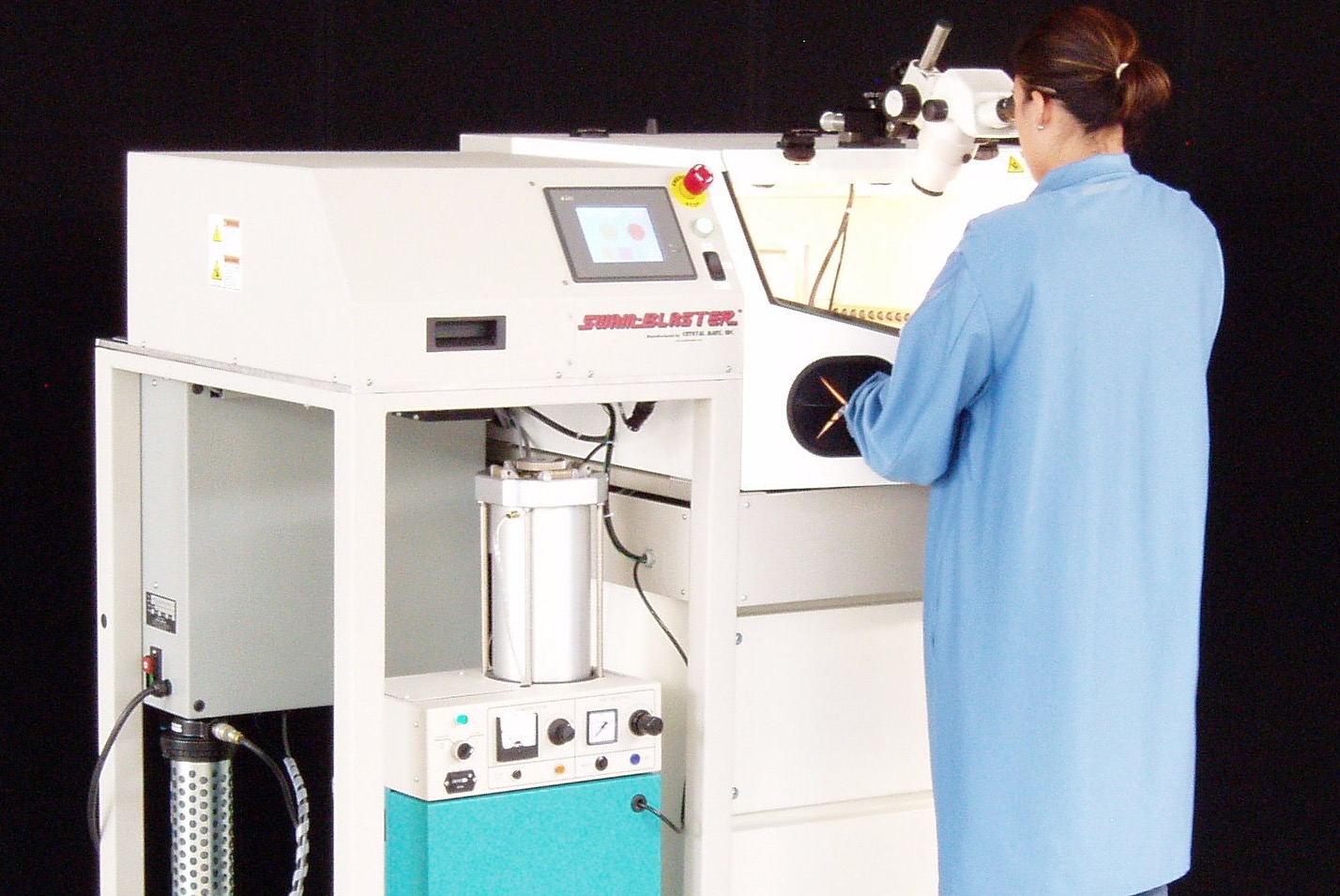
This report details the results and conclusions of an experimental evaluation of a micro abrasive blasting technique to remove urethane and parylene conformal coatings from printed wiring assemblies. This technique is being evaluated as a replacement for solvent based systems. The SWAM BLASTER coating removal system from Crystal Mark, Inc. was used. Four blast medias were evaluated using a total of 20 printed wiring assemblies. The effectiveness of the microblasting technique was evaluated to determine the electrostatic potential generated at the surface and any visible board damage. The microblaster effectively removed the conformal coatings from all printed wiring assemblies evaluated. However, the concerns of electrostatic potential generation and the effects of a number of variables which were not addressed in this study, needs further research prior to being acceptable for space flight applications.
Background
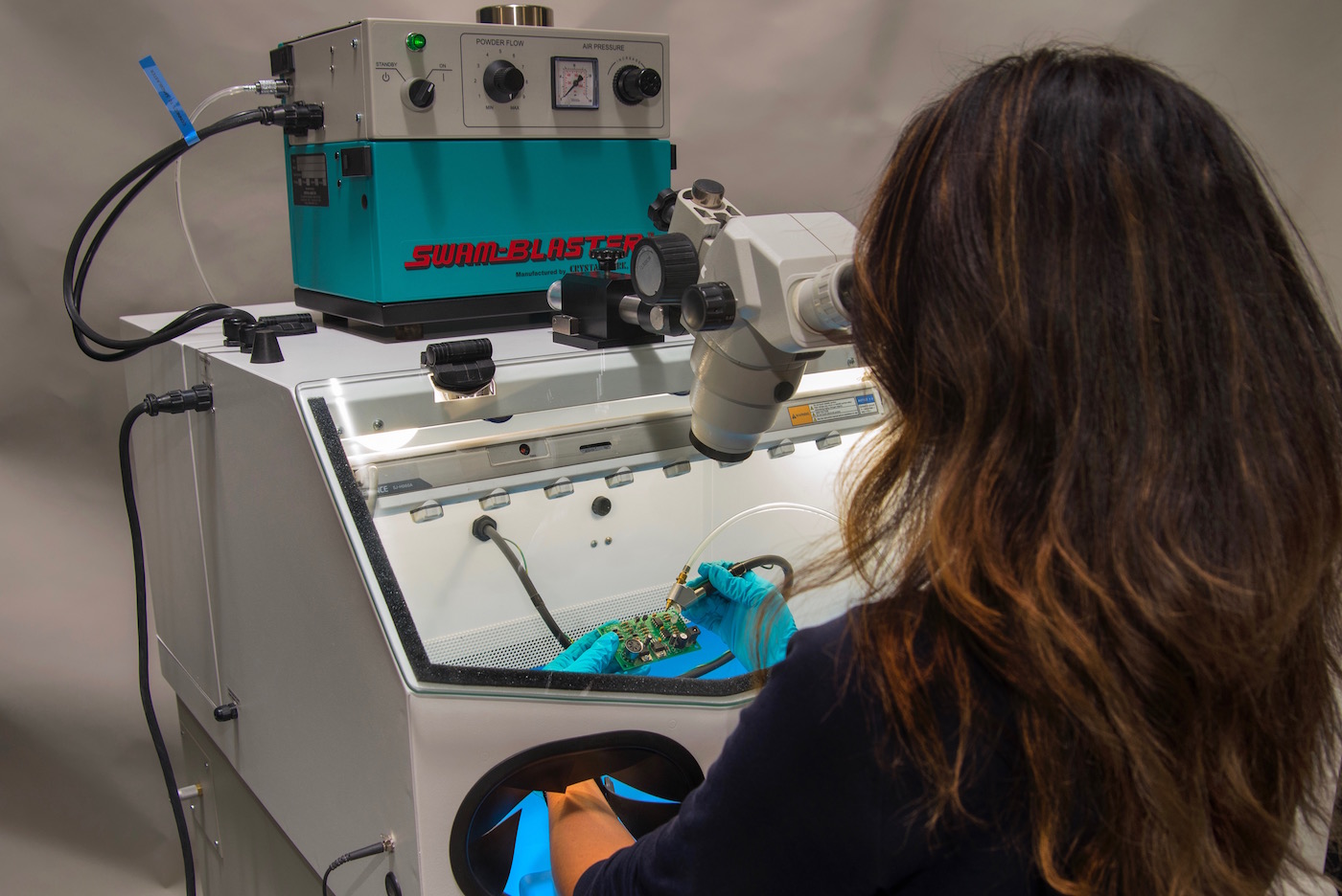
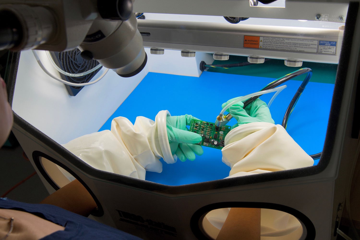
Conformal coatings are required on printed wiring assemblies (PWAs) used for space light applications to provide protection and to extend the life of the assemblies in harsh environments. There are four major types of coating materials, each developed to suit specific applications. These are: acrylics, urethanes, silicones and parylenes. Depending upon the type of coating material and product requirements, conformal coating may be applied by dipping, brushing, spraying, dispensing or chemical vapor deposition. In order to rework or repair parts on PWAs, the conformal coating must be removed, either entirely or in specific areas. The most commonly used methods for removal involve thermal, chemical, mechanical and micro abrasive processes. Recent environmental regulations such as the Montreal Protocol and Clean Air Act have had a significant impact on solvent based conformal coating removal processes, particularly with regard to control of volatile organic compounds (VOCs) and ozone depleting chemicals (ODCs). Equipment suppliers for coating removal systems have responded by developing environmentally acceptable methods. The micro abrasive blasting technique offers a fast, cost-effective, easy to control and environmentally friendly non-solvent based method to remove conformal coatings. The system can remove conformal coatings from a single test node, an axial leaded component, a through-hole integrated circuit (IC), a surface mount component (SMC) or an entire printed circuit board (PCB). In the micro abrasive blasting process, a precise mixture of dry air or an inert gas and an abrasive media is propelled through a tiny nozzle attached to a stylus which is either hand held or mounted on an automated system. This allows the mixture to be pinpointed at the target area of the conformal coating to be removed. A vacuum system continuously removes the used materials and channels them through a filtration system for disposal. The process is conducted within an enclosed anti-static chamber and features grounding devices to dissipate electrostatic potential. Micro abrasive systems inherently generate static electricity as the high velocity particles impinge on the surfaces. The voltage generated at the area of impact can cause electrostatic discharge (ESD) damage to the parts and electrical circuits on a PWA. The current trend in the electronics industry towards higher speed, greater packaging density and lower power consumption has increased static sensitivity so that new techniques emerging in the field of coating technology need more stringent attention than ever before. An ideal blast media in a coating removal process would be the one which will not generate voltage greater than the ESD susceptibility of a particular device on a PWA or damage the board assembly, and is environmentally acceptable.
Conformal Coating Removal
Methodology
The objective of this study is to determine the effectiveness of the micro abrasive blasting technique to remove the conformal coatings from printed circuit boards and assemblies. This evaluation includes determination of the level of electrostatic voltage by measuring the surface voltage generated at the point of contact. It also includes assessing any physical damage caused by the technique. The experimental characterization includes the effects of variables such as type of conformal coating, cutting media, and system parameters on the conformal coating removal process.
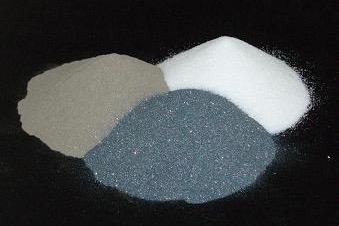
Two types of conformal coatings were evaluated. These included urethane and parylene (parylene type C) conformal coatings with 4 mil and 1 mil nominal thicknesses respectively. The PWAs were non-functional. A total of four blast medias were selected. These included: wheat starch, sodium bicarbonate, plastic beads and glass beads.
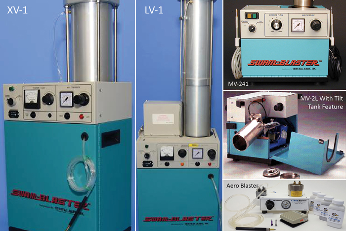
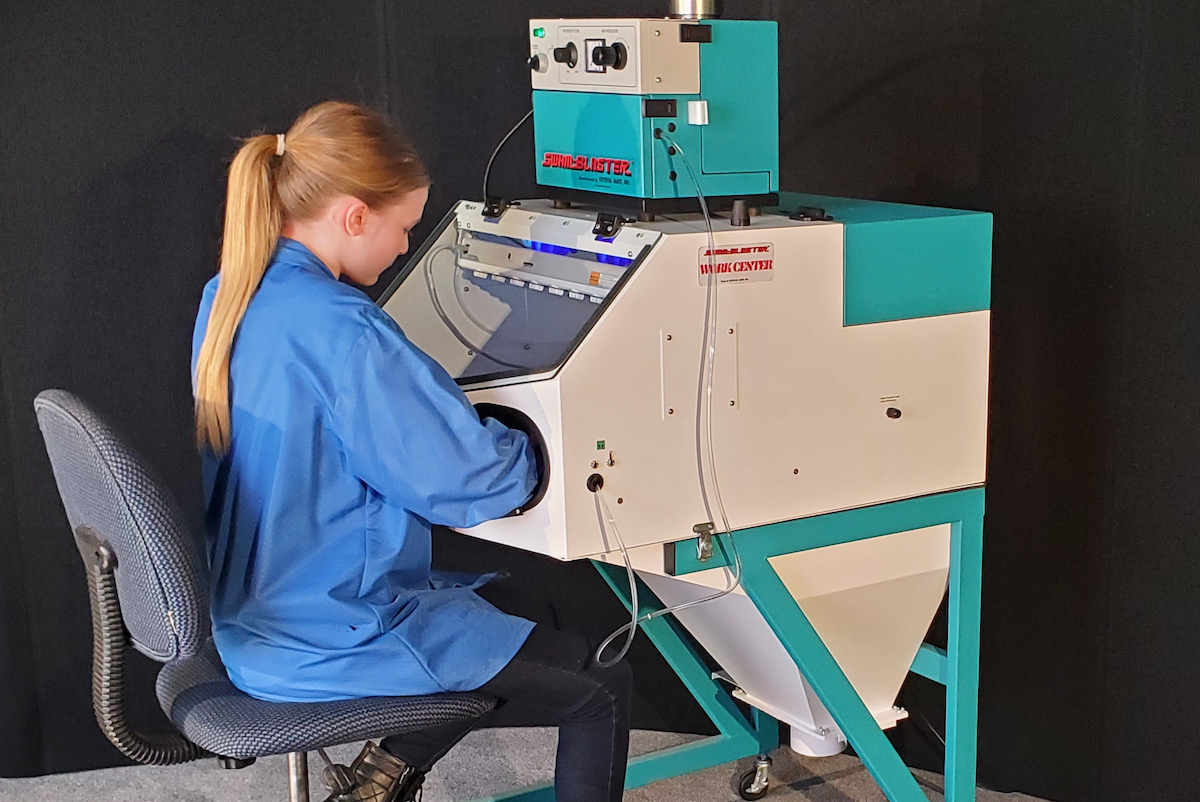
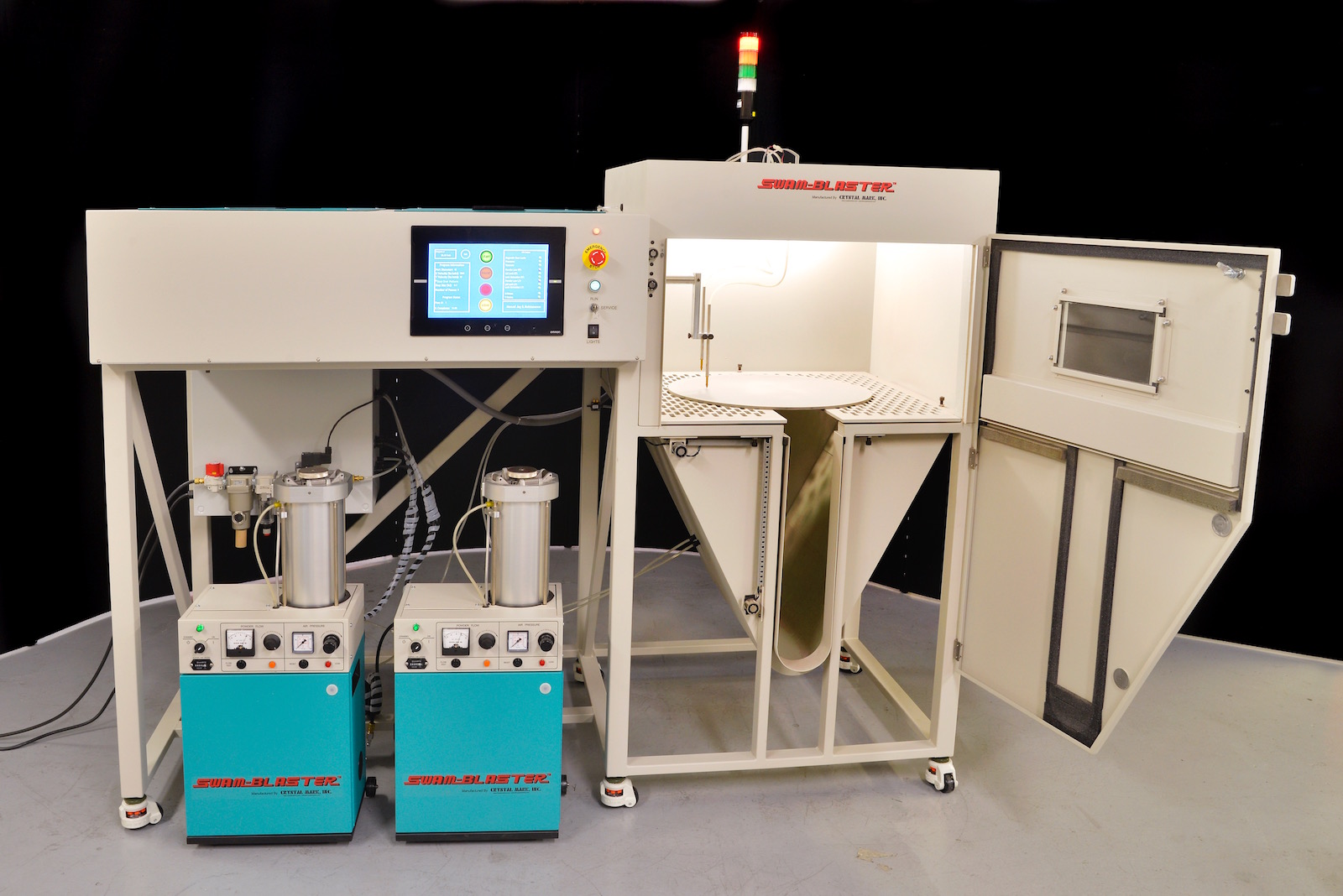
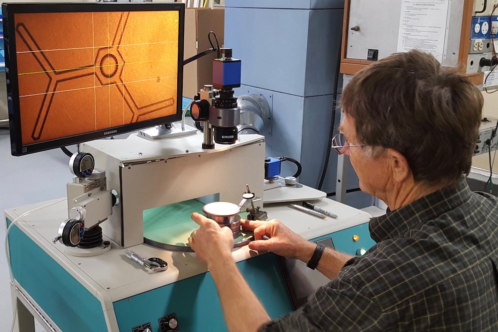
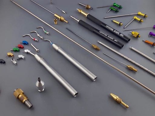
A SWAM BLASTER Model MV-1 made by Crystal Mark, Inc. Glendale, California was used throughout this study. A Monroe Electronics Model 244 Isoprobe Electrostatic Voltmeter was used to monitor ESD voltages generated at the surfaces. This electrostatic voltmeter used an end-viewing miniature probe (Model 1017) with inert gas purging capability. Cleaninert gas is purged through the sensing aperture preventing contamination by the blast medias in the vicinity of the electrode for greater stability of measurement. The probe measures the surface voltage with high accuracy (0.1%) and a test response speed < 3mS throughout a range of ± 3 kilovolts.
The evaluation was performed at the Materials Engineering Laboratory, NASA/GSFC in Greenbelt, Maryland.
Experimental Plan
A total of 20 non-functional PWAs were selected for this evaluation. All PWAs were double sided, 75mm x 125 mm (3″ x 5″) FR4 laminate. These PWAs have been designed for the use by the NASA Training Center for training in hand soldering, surface mount attachment,cleaning and conformal coating applications. This configuration provided a variety of pad geometries and traces adjacent to the blast sites and in close proximity to through-hole parts, flat packs, and other discrete devices (see figure 2 and 3).
A total of five blast sites were selected for monitoring ESD voltage (see figure 2 and 3).
These included:
Experimental Matrix
A total of 20 PWAs were coated with urethane and parylene conformal coatings; ten each. All four blast medias were procured from Crystal Mark, Inc. The specifications of these are listed below:

